Work
Schematics and layouts
Sheets and boards from recent projects, client work and our own.
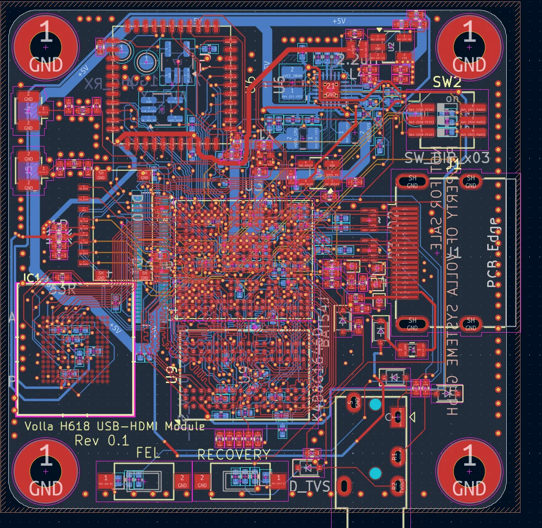
USB-HDMI application module
Layout- Allwinner H618 BGA
- DDR memory
- USB + HDMI
- DIP switches, FEL and recovery buttons
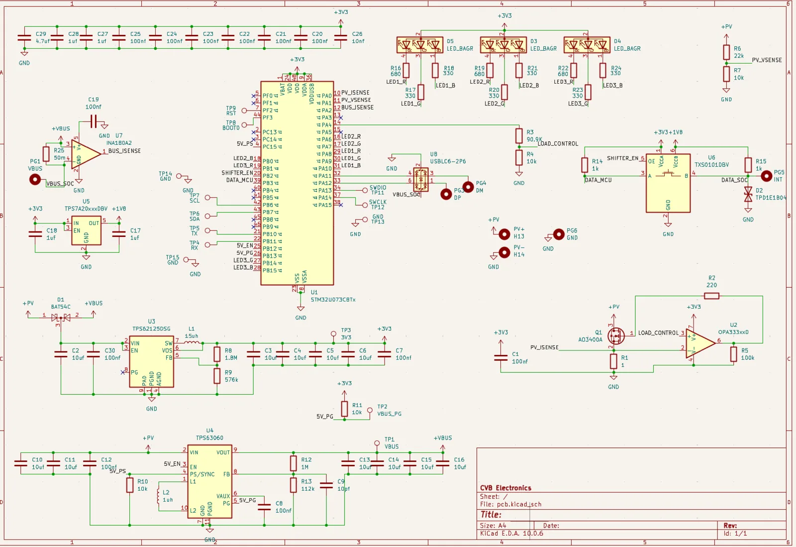
Power path and control
Schematic- STM32U073
- TPS62125 buck, TPS63060 buck-boost
- INA180 current sense, OPA333
- TXS0101 level shifter, USBLC6 ESD
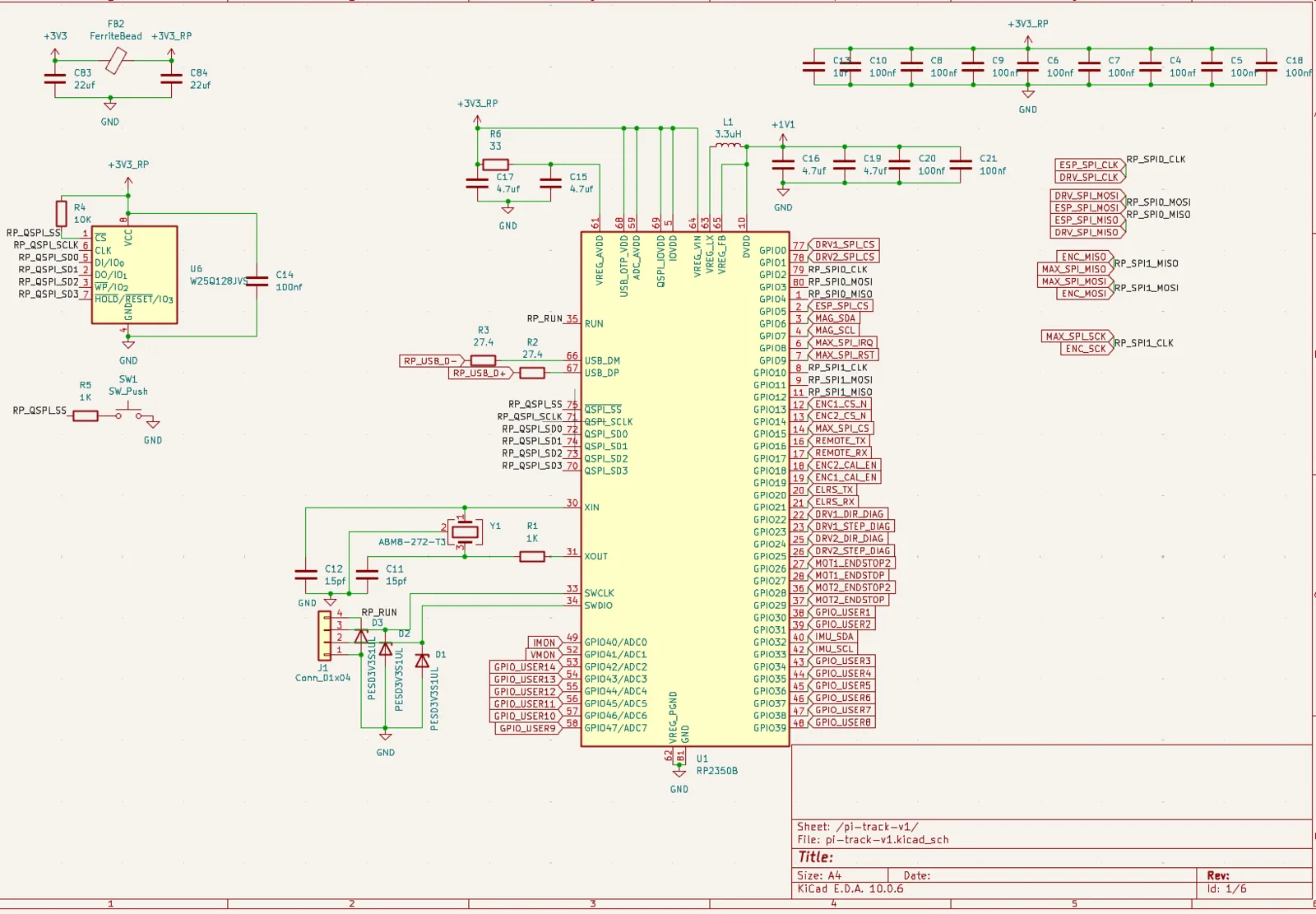
Motion controller
Schematic- RP2350B
- W25Q128 QSPI flash
- SPI to two stepper drivers
- Encoder, IMU and magnetometer buses
- ELRS radio UART
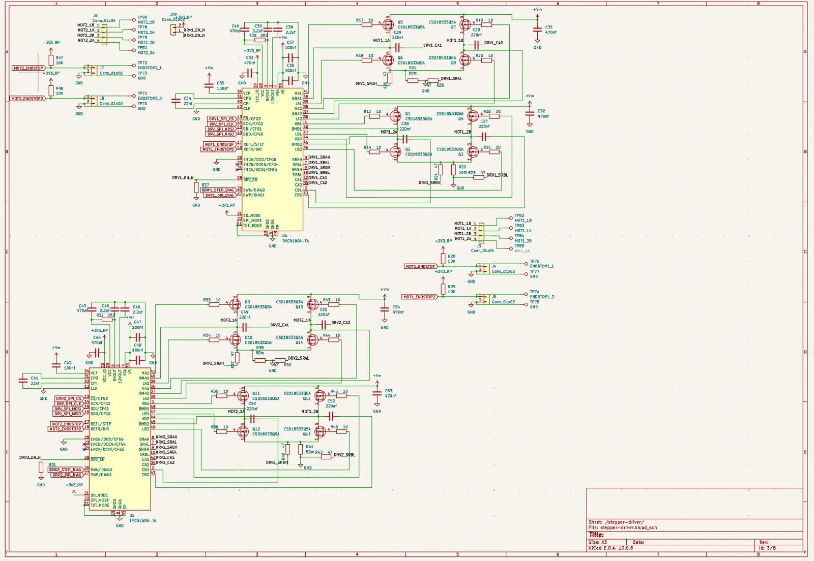
Dual stepper power stage
Schematic- 2× TMC5160A
- CSD18533Q5A external bridges
- 50 mΩ sense resistors
- Endstop input per axis
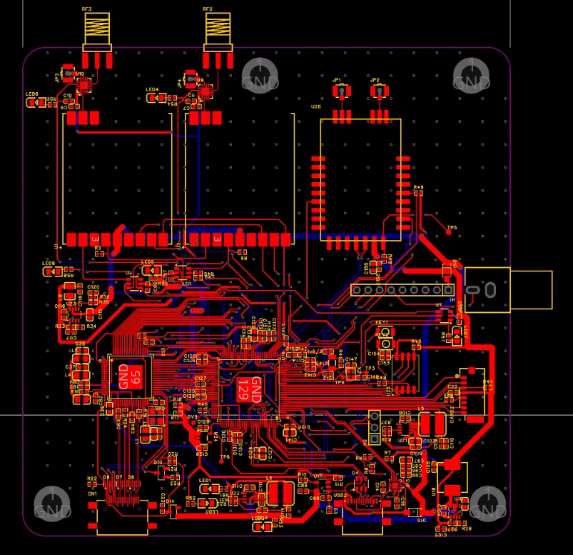
Wireless board
Layout- Two edge-mounted RF connectors
- Shielded module footprint
- USB connector
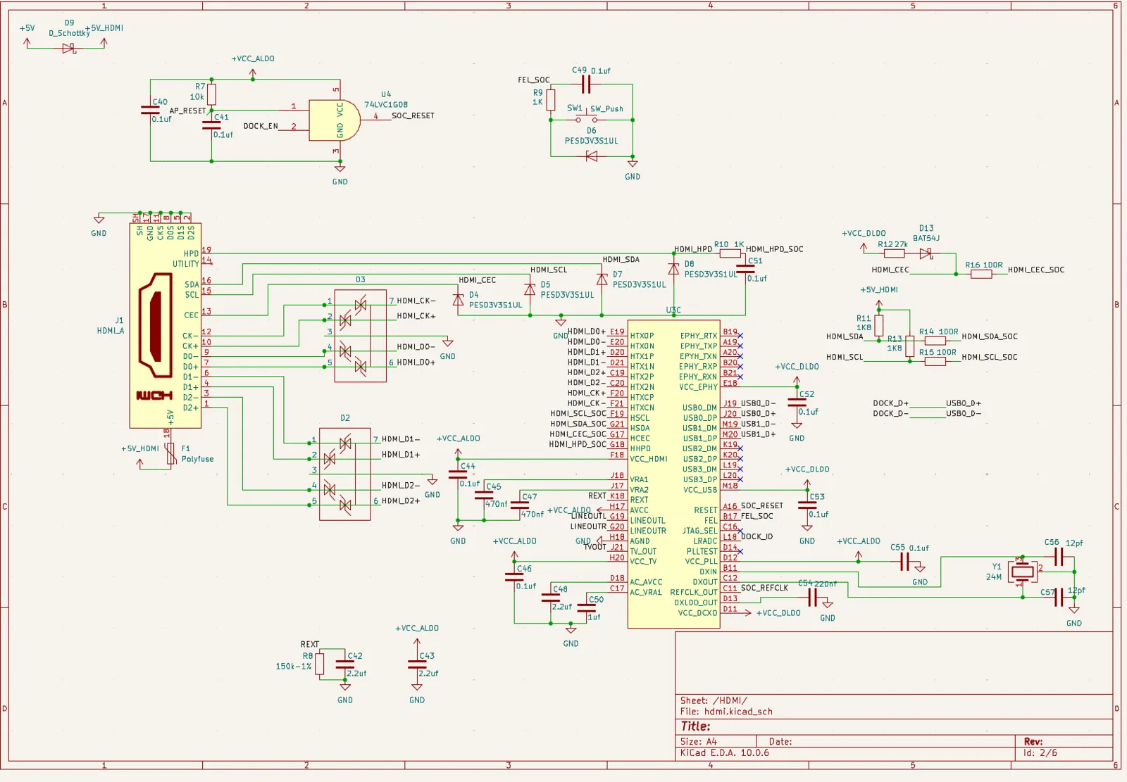
HDMI interface
Schematic- HDMI type-A input
- PESD3V3S1UL ESD on each pair
- Polyfuse on +5 V
- 74LVC1G08 reset gating
- 24 MHz reference
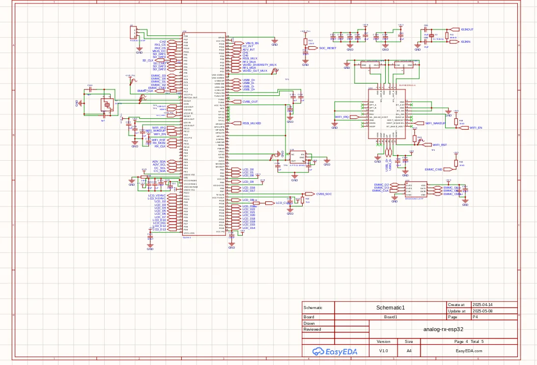
SoC carrier
Schematic- eMMC
- Wi-Fi and Bluetooth module
- Parallel LCD bus
- USB
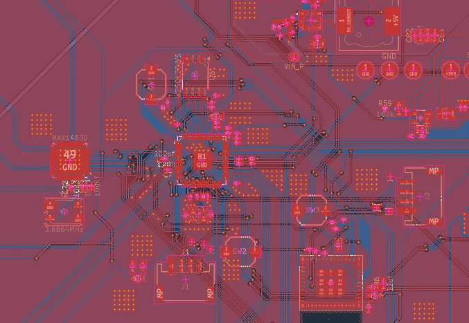
Layout detail
Layout- MAX14830 quad UART
- 3.6864 MHz crystal
Click any image for the full-size view. Drawn in KiCad and EasyEDA. Sources and manufacturing files are handed over at the end of every project.
Need work like this?
Describe what the board has to do and you get a straight answer on feasibility, cost and timeline before anything is committed.